R1000AX Specifications
Order R1000AX and other modules here.
Overview
R1000AX is a base board for the JuicyBoard platform. It includes 15 feature slots, efficient switching regulators with 5V and 3.3V outputs, power monitoring and safety features.
Architecture
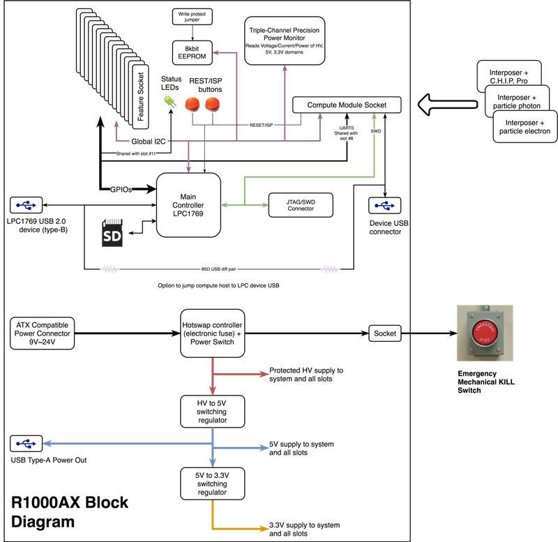
This is a block diagram of the board
Design Source Files
Design source files are available on GitHub.
Slot Distribution and Pin Assignment
| Pin Name | LQFP100 Pin | GPIO | F1 | F2 | F3 | Juicy Function | Socket Number | Pin Order in Socket |
| P0[28]/SCL0/USB_SCL | 24 | P0[28] | Reserved SCL0 | I2C0 | ||||
| P0[27]/SDA0/USB_SDA | 25 | P0[27] | Reserved SDA0 | |||||
| P0[24]/AD0[1]/I2SRX_WS/CAP3[1] | 8 | P0[24] | AD0[1] | ADC | 1 | 1 | ||
| P0[23]/AD0[0]/I2SRX_CLK/CAP3[0] | 9 | P0[23] | AD0[0] | ADC | 2 | |||
| P1[31]/SCK1/AD0[5] | 20 | P1[31] | SCK1 | AD0[5] | ADC | 3 | ||
| P1[30]/VBUS/AD0[4] | 21 | P1[30] | VBUS | AD0[4] | ADC | 4 | ||
| P2[3]/PWM1[4]/DCD1/TRACEDATA[2] | 70 | P2[3] | PWM1[4] | PWM | 2 | 1 | ||
| P2[2]/PWM1[3]/CTS1/TRACEDATA[3] | 73 | P2[2] | PWM1[3] | PWM | 2 | |||
| P2[1]/PWM1[2]/RXD1 | 74 | P2[1] | PWM1[2] | RXD1 | PWM | 3 | ||
| P2[0]/PWM1[1]/TXD1 | 75 | P2[0] | PWM1[1] | TXD1 | PWM | 4 | ||
| P1[25]/MCOA1/MAT1[1] | 39 | P1[25] | GPIO | 3 | 1 | |||
| P1[24]/MCI2/PWM1[5]/MOSI0 | 38 | P1[24] | GPIO | 2 | ||||
| P1[23]/MCI1/PWM1[4]/MISO0 | 37 | P1[23] | GPIO | 3 | ||||
| P1[22]/MCOB0/USB_PWRD/MAT1[0] | 36 | P1[22] | GPIO | 4 | ||||
| P1[29]/MCOB2/PCAP1[1]/MAT0[1] | 45 | P1[29] | GPIO | 4 | 1 | |||
| P1[28]/MCOA2/PCAP1[0]/MAT0[0] | 44 | P1[28] | GPIO | 2 | ||||
| P1[27]/CLKOUT/USB_OVRCR/CAP0[1] | 43 | P1[27] | GPIO | 3 | ||||
| P1[26]/MCOB1/PWM1[6]/CAP0[0] | 40 | P1[26] | GPIO | 4 | ||||
| P0[0]/RD1/TXD3/SDA1 | 46 | P0[0] | UART2/I2C2 | 5 | 1 | |||
| P0[1]/TD1/RXD3/SCL1 | 47 | P0[1] | UART2/I2C2 | 2 | ||||
| P0[11]/RXD2/SCL2/MAT3[1] | 49 | P0[11] | RXD2 | SCL2 | UART2/I2C2 | 3 | ||
| P0[10]/TXD2/SDA2/MAT3[0] | 48 | P0[10] | TXD2 | SDA2 | UART2/I2C2 | 4 | ||
| P2[13]/EINT3/I2STX_SDA | 50 | P2[13] | GPIO | 6 | 1 | |||
| P2[12]/EINT2/I2STX_WS | 51 | P2[12] | GPIO | 2 | ||||
| P2[11]/EINT1/I2STX_CLK | 52 | P2[11] | GPIO | 3 | ||||
| P3[25]/MAT0[0]/PWM1[2] | 27 | P3[25] | GPIO | 4 | ||||
| P0[22]/RTS1/TD1 | 56 | P0[22] | I2C1 | 7 | 1 | |||
| P0[21]/RI1/RD1 | 57 | P0[21] | I2C1 | 2 | ||||
| P0[20]/DTR1/SCL1 | 58 | P0[20] | SCL1 | I2C1 | 3 | |||
| P0[19]/DSR1/SDA1 | 59 | P0[19] | SDA1 | I2C1 | 4 | |||
| P0[25]/AD0[2]/I2SRX_SDA/TXD3 | 7 | P0[25] | AD0[2] | TXD3 | ADC/UART0 | 8 | 1 | |
| P0[26]/AD0[3]/AOUT/RXD3 | 6 | P0[26] | AD0[3] | AOUT | RXD3 | ADC/UART0 | 2 | |
| P0[3]/RXD0/AD0[6] | 99 | P0[3] | RXD0 | AD0[6] | ADC/UART0 | 3 | ||
| P0[2]/TXD0/AD0[7] | 98 | P0[2] | TXD0 | AD0[7] | ADC/UART0 | 4 | ||
| P0[18]/DCD1/MOSI0/MOSI | 60 | P0[18] | MOSI0 | SPI0 | 9 | 1 | ||
| P0[17]/CTS1/MISO0/MISO | 61 | P0[17] | MISO0 | SPI0 | 2 | |||
| P0[16]/RXD1/SSEL0/SSEL | 63 | P0[16] | SSEL0 | SSEL | SPI0 | 3 | ||
| P0[15]/TXD1/SCK0/SCK | 62 | P0[15] | SCK0 | SPI0 | 4 | |||
| P2[7]/RD2/RTS1 | 66 | P2[7] | GPIO | 10 | 1 | |||
| P2[6]/PCAP1[0]/RI1/TRACECLK | 67 | P2[6] | GPIO | 2 | ||||
| P2[5]/PWM1[6]/DTR1/TRACEDATA[0] | 68 | P2[5] | PWM1[6] | GPIO | 3 | |||
| P2[4]/PWM1[5]/DSR1/TRACEDATA[1] | 69 | P2[4] | PWM1[5] | GPIO | 4 | |||
| P1[21]/MCABORT/PWM1[3]/SSEL0 | 35 | P1[21] | LED/GPIO | 11 | 1 | |||
| P1[20]/MCI0/PWM1[2]/SCK0 | 34 | P1[20] | LED/GPIO | 2 | ||||
| P1[19]/MCOA0/USB_PPWR/CAP1[1] | 33 | P1[19] | LED/GPIO | 3 | ||||
| P1[18]/USB_UP_LED/PWM1[1]/CAP1[0] | 32 | P1[18] | LED/GPIO | 4 | ||||
| P0[5]/I2SRX_WS/TD2/CAP2[1] | 80 | P0[5] | UART3 | 12 | 1 | |||
| P0[4]/I2SRX_CLK/RD2/CAP2[0] | 81 | P0[4] | UART3 | 2 | ||||
| P4[29]/TX_MCLK/MAT2[1]/RXD3 | 85 | P4[29] | RXD3 | UART3 | 3 | |||
| P4[28]/RX_MCLK/MAT2[0]/TXD3 | 82 | P4[28] | TXD3 | UART3 | 4 | |||
| P2[8]/TD2/TXD2 | 65 | P2[8] | ENET0 | 13 | 1 | |||
| P3[26]/STCLK/MAT0[1]/PWM1[3] | 26 | P3[26] | ENET0 | 2 | ||||
| P1[0]/ENET_TXD0 | 95 | P1[0] | ENET_TXD0 | ENET0 | 3 | |||
| P1[1]/ENET_TXD1 | 94 | P1[1] | ENET_TXD1 | ENET0 | 4 | |||
| P1[17]/ENET_MDIO | 86 | P1[17] | ENET_MDIO | ENET1 | 14 | 1 | ||
| P1[16]/ENET_MDC | 87 | P1[16] | ENET_MDC | ENET1 | 2 | |||
| P1[15]/ENET_REF_CLK | 88 | P1[15] | ENET_REF_CLK | ENET1 | 3 | |||
| P1[14]/ENET_RX_ER | 89 | P1[14] | ENET_RX_ER | ENET1 | 4 | |||
| P1[10]/ENET_RXD1 | 90 | P1[10] | ENET_RXD1 | ENET2 | 15 | 1 | ||
| P1[9]/ENET_RXD0 | 91 | P1[9] | ENET_RXD0 | ENET2 | 2 | |||
| P1[8]/ENET_CRS | 92 | P1[8] | ENET_CRS | ENET2 | 3 | |||
| P1[4]/ENET_TX_EN | 93 | P1[4] | ENET_TX_EN | ENET2 | 4 | |||
| P2[10]/EINT0/NMI | 53 | P2[10] | ISP_BOOT | ISP/MRESET | ||||
| P0[9]/I2STX_SDA/MOSI1/MAT2[3] | 76 | P0[9] | Reserved SDC MOSI1 | SD Card | ||||
| P0[8]/I2STX_WS/MISO1/MAT2[2] | 77 | P0[8] | Reserved SDC MISO1 | |||||
| P0[7]/I2STX_CLK/SCK1/MAT2[1] | 78 | P0[7] | Reserved SDC SCK1 | |||||
| P0[6]/I2SRX_SDA/SSEL1/MAT2[0] | 79 | P0[6] | Reserved SDC SSEL1 | |||||
| P0[29]/USB_D+ | 29 | P0[29] | Reserved USB_D+ | USB | ||||
| P0[30]/USB_D | 30 | P0[30] | Reserved USB_D | |||||
| P2[9]/USB_CONNECT/RXD2 | 64 | P2[9] | Reserved, USB P-drive | USB DFU P |
Board Interfaces
Power
USB Data
Hot-swap Controller and System Protection
Power Tree
System Power Monitoring
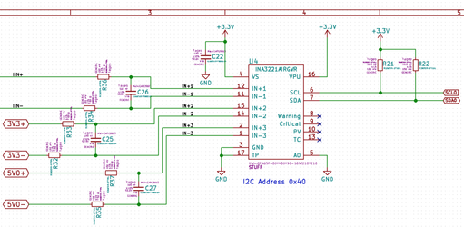
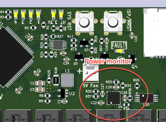
R1000AX includes an INA3221 high side supply monitor from TI. It monitors the high voltage, 5V and 3.3V domains.
| INA3221 Channel # | Voltage Domain | Operating Range |
|---|---|---|
| 1 | High voltage | 9 ~ 24V |
| 2 | +5V | 4.5v~5.5V |
| 3 | +3.3V | 3V~3.6V |
EEPROM For Storing NV Configuration Data
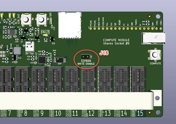
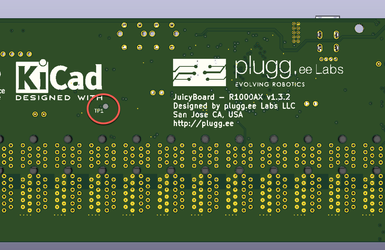
R1000AX includes a small 8kbit EEPROM that can be used to store critical configuration data outside the MCU flash memory. This is useful for tracking changes, serial number ... etc. By default the EEPROM is write protected, the user enable write by 2 ways
| Short J18 with a jumper | |
| Connect TP1 on the bottom of the board to ground. This is useful for automated test setups |
Compute Module
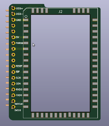
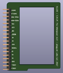
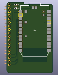
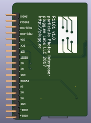
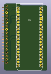
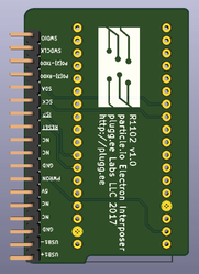
Currently there are 3 interposer designs that allow mounting a particle Electron, Photon or a C.H.I.P. Pro. Interposer board numbers are
| # | Description | Module to PCB Mounting | Top View | Bottom View |
|---|---|---|---|---|
| R1100 | C.H.I.P. Pro Interposer with Host USB 2.0 | SMT soldered | ||
| R1101 | particle Photon Interposer | SMT soldered | ||
| R1102 | particle Electron Interposer | Through-hole header |
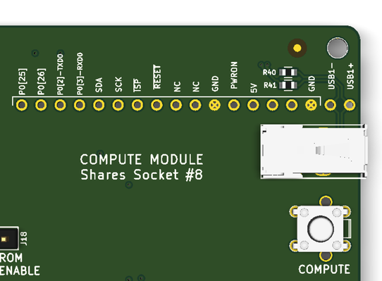
The compute module connects to the following signals on R1000AX:
| R1000AX Signal Name | Description | Polarity | Type | Photon | Electron | C.H.I.P. Pro |
|---|---|---|---|---|---|---|
| !RESET | LPC1769 reset pin | Active Low | Open Drain | A5 | A5 | PB2/SPDIF-DO/PWM0 |
| ISP/Module Reset | LPC1769 boot pin AND module reset | Active Low | Open Drain | A4 | A4 | PG13/EINT13/PWM1 |
| SWDCLK | LPC1769 SWD clock | - | Push-Pull, tie low or leave floating for normal operation | A3 | A3 | PD4/UART2-CTS |
| SWDIO | LPC1769 SWD data | - | Push-Pull, leave floating for normal operation | A2 | A2 | PD5/UART2-RTS |
| RXD0 | LPC1769 UART0 RX pin | - | Input to LPC1769, output from compute module | TX | TX | PD2/UART2-TX |
| TXD0 | LPC1769 UART0 TX pin | - | Output from LPC1769, input to compute module | RX | RX | PD3/UART2-RX |
| COMPUTE_USB+/- | Host USB from compute module (C.H.I.P. Pro) | Differential Pair | USB 2.0 | - | - | USB0-UDM0/UDP0 |
| +5V | 5V supply from R1000AX to power compute module | - | Power pin | VIN | VIN | CHG-IN |
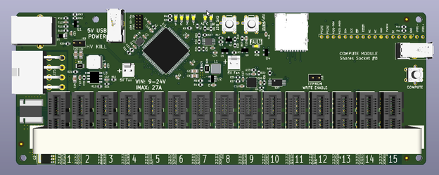
This is the footprint for the compute module
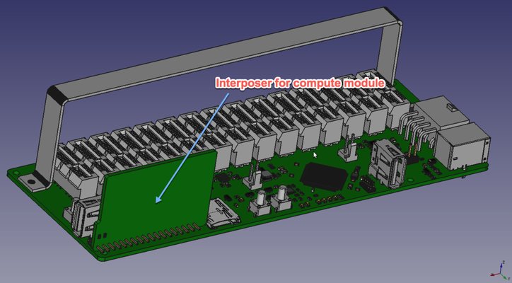
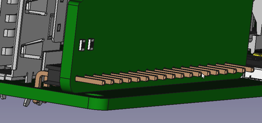
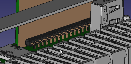
The interposer is mounted on R1000AX using a right angled 100mil header connector
Mechanical
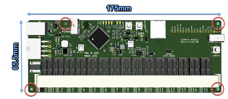
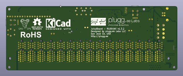
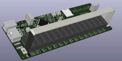
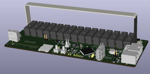
R1000AX PCB has dimensions of 175mm x 65.5mm, it includes 4x M3 mounting holes in the indicated positions.
.png?version=1&modificationDate=1491605935131&cacheVersion=1&api=v2&width=580&height=400)
