Overview
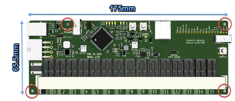
R1000AX is a base board for the JuicyBoard platform. It includes 15 feature slots, efficient switching regulators with 5V and 3.3V outputs, power monitoring and safety features.
Architecture
This is a block diagram of the board

Design Source Files
Design source files are available on GitHub.
Slot Distribution and Pin Assignment
| Pin Name | LQFP100 Pin | GPIO | F1 | F2 | F3 | Juicy Function | Socket Number | Pin Order in Socket |
| P0[28]/SCL0/USB_SCL | 24 | P0[28] | Reserved SCL0 | I2C0 | ||||
| P0[27]/SDA0/USB_SDA | 25 | P0[27] | Reserved SDA0 | |||||
| P0[24]/AD0[1]/I2SRX_WS/CAP3[1] | 8 | P0[24] | AD0[1] | ADC | 1 | 1 | ||
| P0[23]/AD0[0]/I2SRX_CLK/CAP3[0] | 9 | P0[23] | AD0[0] | ADC | 2 | |||
| P1[31]/SCK1/AD0[5] | 20 | P1[31] | SCK1 | AD0[5] | ADC | 3 | ||
| P1[30]/VBUS/AD0[4] | 21 | P1[30] | VBUS | AD0[4] | ADC | 4 | ||
| P2[3]/PWM1[4]/DCD1/TRACEDATA[2] | 70 | P2[3] | PWM1[4] | PWM | 2 | 1 | ||
| P2[2]/PWM1[3]/CTS1/TRACEDATA[3] | 73 | P2[2] | PWM1[3] | PWM | 2 | |||
| P2[1]/PWM1[2]/RXD1 | 74 | P2[1] | PWM1[2] | RXD1 | PWM | 3 | ||
| P2[0]/PWM1[1]/TXD1 | 75 | P2[0] | PWM1[1] | TXD1 | PWM | 4 | ||
| P1[25]/MCOA1/MAT1[1] | 39 | P1[25] | GPIO | 3 | 1 | |||
| P1[24]/MCI2/PWM1[5]/MOSI0 | 38 | P1[24] | GPIO | 2 | ||||
| P1[23]/MCI1/PWM1[4]/MISO0 | 37 | P1[23] | GPIO | 3 | ||||
| P1[22]/MCOB0/USB_PWRD/MAT1[0] | 36 | P1[22] | GPIO | 4 | ||||
| P1[29]/MCOB2/PCAP1[1]/MAT0[1] | 45 | P1[29] | GPIO | 4 | 1 | |||
| P1[28]/MCOA2/PCAP1[0]/MAT0[0] | 44 | P1[28] | GPIO | 2 | ||||
| P1[27]/CLKOUT/USB_OVRCR/CAP0[1] | 43 | P1[27] | GPIO | 3 | ||||
| P1[26]/MCOB1/PWM1[6]/CAP0[0] | 40 | P1[26] | GPIO | 4 | ||||
| P0[0]/RD1/TXD3/SDA1 | 46 | P0[0] | UART2/I2C2 | 5 | 1 | |||
| P0[1]/TD1/RXD3/SCL1 | 47 | P0[1] | UART2/I2C2 | 2 | ||||
| P0[11]/RXD2/SCL2/MAT3[1] | 49 | P0[11] | RXD2 | SCL2 | UART2/I2C2 | 3 | ||
| P0[10]/TXD2/SDA2/MAT3[0] | 48 | P0[10] | TXD2 | SDA2 | UART2/I2C2 | 4 | ||
| P2[13]/EINT3/I2STX_SDA | 50 | P2[13] | GPIO | 6 | 1 | |||
| P2[12]/EINT2/I2STX_WS | 51 | P2[12] | GPIO | 2 | ||||
| P2[11]/EINT1/I2STX_CLK | 52 | P2[11] | GPIO | 3 | ||||
| P3[25]/MAT0[0]/PWM1[2] | 27 | P3[25] | GPIO | 4 | ||||
| P0[22]/RTS1/TD1 | 56 | P0[22] | I2C1 | 7 | 1 | |||
| P0[21]/RI1/RD1 | 57 | P0[21] | I2C1 | 2 | ||||
| P0[20]/DTR1/SCL1 | 58 | P0[20] | SCL1 | I2C1 | 3 | |||
| P0[19]/DSR1/SDA1 | 59 | P0[19] | SDA1 | I2C1 | 4 | |||
| P0[25]/AD0[2]/I2SRX_SDA/TXD3 | 7 | P0[25] | AD0[2] | TXD3 | ADC/UART0 | 8 | 1 | |
| P0[26]/AD0[3]/AOUT/RXD3 | 6 | P0[26] | AD0[3] | AOUT | RXD3 | ADC/UART0 | 2 | |
| P0[3]/RXD0/AD0[6] | 99 | P0[3] | RXD0 | AD0[6] | ADC/UART0 | 3 | ||
| P0[2]/TXD0/AD0[7] | 98 | P0[2] | TXD0 | AD0[7] | ADC/UART0 | 4 | ||
| P0[18]/DCD1/MOSI0/MOSI | 60 | P0[18] | MOSI0 | SPI0 | 9 | 1 | ||
| P0[17]/CTS1/MISO0/MISO | 61 | P0[17] | MISO0 | SPI0 | 2 | |||
| P0[16]/RXD1/SSEL0/SSEL | 63 | P0[16] | SSEL0 | SSEL | SPI0 | 3 | ||
| P0[15]/TXD1/SCK0/SCK | 62 | P0[15] | SCK0 | SPI0 | 4 | |||
| P2[7]/RD2/RTS1 | 66 | P2[7] | GPIO | 10 | 1 | |||
| P2[6]/PCAP1[0]/RI1/TRACECLK | 67 | P2[6] | GPIO | 2 | ||||
| P2[5]/PWM1[6]/DTR1/TRACEDATA[0] | 68 | P2[5] | PWM1[6] | GPIO | 3 | |||
| P2[4]/PWM1[5]/DSR1/TRACEDATA[1] | 69 | P2[4] | PWM1[5] | GPIO | 4 | |||
| P1[21]/MCABORT/PWM1[3]/SSEL0 | 35 | P1[21] | LED/GPIO | 11 | 1 | |||
| P1[20]/MCI0/PWM1[2]/SCK0 | 34 | P1[20] | LED/GPIO | 2 | ||||
| P1[19]/MCOA0/USB_PPWR/CAP1[1] | 33 | P1[19] | LED/GPIO | 3 | ||||
| P1[18]/USB_UP_LED/PWM1[1]/CAP1[0] | 32 | P1[18] | LED/GPIO | 4 | ||||
| P0[5]/I2SRX_WS/TD2/CAP2[1] | 80 | P0[5] | UART3 | 12 | 1 | |||
| P0[4]/I2SRX_CLK/RD2/CAP2[0] | 81 | P0[4] | UART3 | 2 | ||||
| P4[29]/TX_MCLK/MAT2[1]/RXD3 | 85 | P4[29] | RXD3 | UART3 | 3 | |||
| P4[28]/RX_MCLK/MAT2[0]/TXD3 | 82 | P4[28] | TXD3 | UART3 | 4 | |||
| P2[8]/TD2/TXD2 | 65 | P2[8] | ENET0 | 13 | 1 | |||
| P3[26]/STCLK/MAT0[1]/PWM1[3] | 26 | P3[26] | ENET0 | 2 | ||||
| P1[0]/ENET_TXD0 | 95 | P1[0] | ENET_TXD0 | ENET0 | 3 | |||
| P1[1]/ENET_TXD1 | 94 | P1[1] | ENET_TXD1 | ENET0 | 4 | |||
| P1[17]/ENET_MDIO | 86 | P1[17] | ENET_MDIO | ENET1 | 14 | 1 | ||
| P1[16]/ENET_MDC | 87 | P1[16] | ENET_MDC | ENET1 | 2 | |||
| P1[15]/ENET_REF_CLK | 88 | P1[15] | ENET_REF_CLK | ENET1 | 3 | |||
| P1[14]/ENET_RX_ER | 89 | P1[14] | ENET_RX_ER | ENET1 | 4 | |||
| P1[10]/ENET_RXD1 | 90 | P1[10] | ENET_RXD1 | ENET2 | 15 | 1 | ||
| P1[9]/ENET_RXD0 | 91 | P1[9] | ENET_RXD0 | ENET2 | 2 | |||
| P1[8]/ENET_CRS | 92 | P1[8] | ENET_CRS | ENET2 | 3 | |||
| P1[4]/ENET_TX_EN | 93 | P1[4] | ENET_TX_EN | ENET2 | 4 | |||
| P2[10]/EINT0/NMI | 53 | P2[10] | ISP_BOOT | ISP/MRESET | ||||
| P0[9]/I2STX_SDA/MOSI1/MAT2[3] | 76 | P0[9] | Reserved SDC MOSI1 | SD Card | ||||
| P0[8]/I2STX_WS/MISO1/MAT2[2] | 77 | P0[8] | Reserved SDC MISO1 | |||||
| P0[7]/I2STX_CLK/SCK1/MAT2[1] | 78 | P0[7] | Reserved SDC SCK1 | |||||
| P0[6]/I2SRX_SDA/SSEL1/MAT2[0] | 79 | P0[6] | Reserved SDC SSEL1 | |||||
| P0[29]/USB_D+ | 29 | P0[29] | Reserved USB_D+ | USB | ||||
| P0[30]/USB_D | 30 | P0[30] | Reserved USB_D | |||||
| P2[9]/USB_CONNECT/RXD2 | 64 | P2[9] | Reserved, USB P-drive | USB DFU P |
Board Interfaces
Power
USB Data
Hot-swap Controller and System Protection
Power Tree
System Power Monitoring
EEPROM For Storing NV Configuration Data
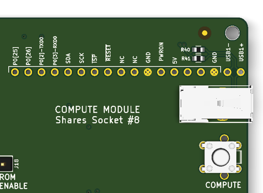
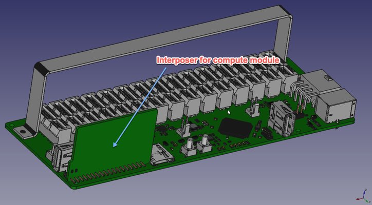
Compute Module
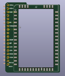
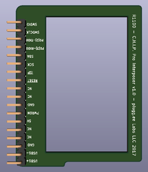
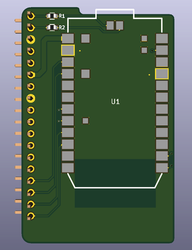
Currently there are 3 interposer designs that allow mounting a particle Electron, Photon or a C.H.I.P. Pro. Interposer board numbers are
| # | Description | Module to PCB Mounting | Top View | Bottom View |
|---|---|---|---|---|
| R1100 | C.H.I.P. Pro Interposer with Host USB 2.0 | SMT soldered |
|
|
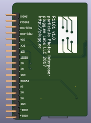
| R1101 | particle Photon Interposer | SMT soldered |
|
|
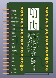
| R1102 | particle Electron Interposer | Through-hole header |
|
|
The compute module connects to the following signals on R1000AX:
| R1000AX Signal Name | Description | Polarity | Type | Photon | Electron | C.H.I.P. Pro |
|---|---|---|---|---|---|---|
| !RESET | LPC1769 reset pin | Active Low | Open Drain | |||
| ISP/Module Reset | LPC1769 boot pin AND module reset | Active Low | Open Drain | |||
| SWDCLK | LPC1769 SWD clock | - | Push-Pull, tie low or leave floating for normal operation | |||
| SWDIO | LPC1769 SWD data | - | Push-Pull, leave floating for normal operation | |||
| RXD0 | LPC1769 UART0 RX pin | - | Input to LPC1769, output from compute module | |||
| TXD0 | LPC1769 UART0 TX pin | - | Output from LPC1769, input to compute module | |||
| COMPUTE_USB+/- | Host USB from compute module (C.H.I.P. Pro) | Differential Pair | USB 2.0 | |||
| +5V | 5V supply from R1000AX to power compute module | - | Power pin |
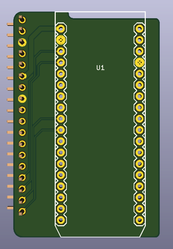
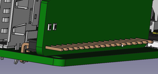
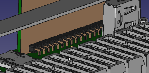
This is the footprint for the compute module
The interposer is mounted on R1000AX using a right angled 100mil header connector
Mechanical
R1000AX PCB has dimensions of 175mm x 65.5mm, it includes 4x M3 mounting holes in the indicated positions.